 Verified PCB & PCBA manufacturing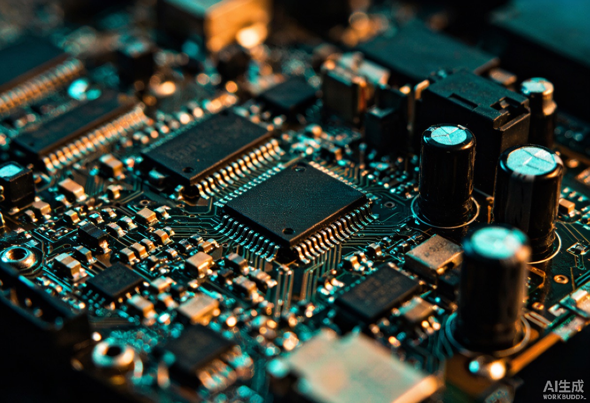
PCB
PCB Manufacturing
- Multilayer and controlled-impedance PCB
- High-TG, heavy-copper and aluminum options
- HDI, flexible and specialty builds by review
Verified PCB & PCBA manufacturer
Engineered. Controlled. Verified.
VeriPCB provides PCB fabrication and PCBA assembly with engineering review, controlled manufacturing processes and documented quality verification—from prototype development to recurring production.
Need an NDA first? Ask before sending confidential design files.
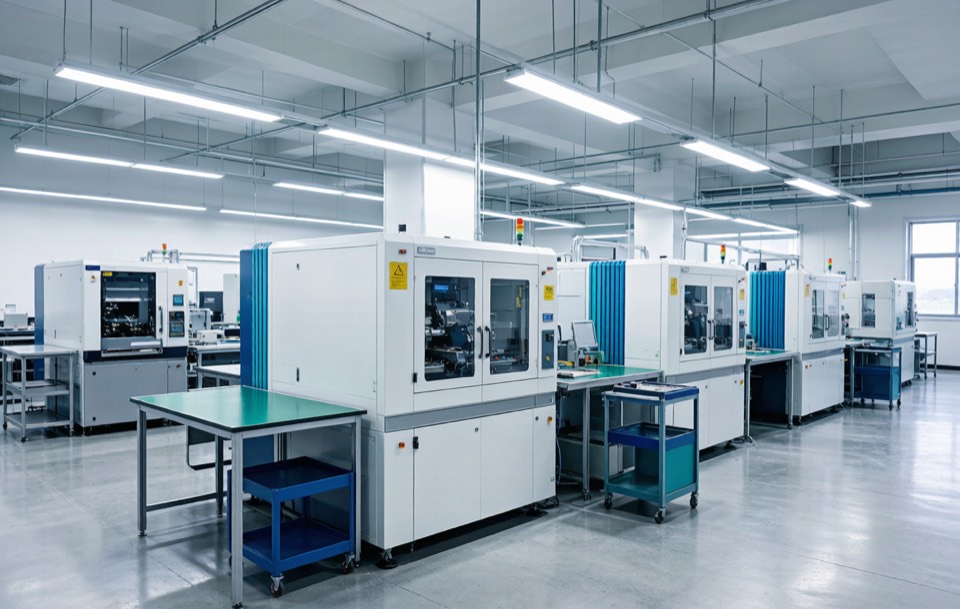
Manufacturing first
Start with the question every engineering buyer asks first: can this manufacturer build, assemble and verify my product?
PCB
PCBA

NPI
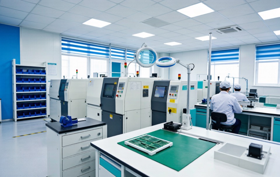
PRODUCTION
Capability overview
| Manufacturing area | Typical options | Verified before order |
|---|---|---|
| PCB fabrication | Multilayer, HDI, high-TG, heavy copper, aluminum, flex and controlled impedance | Stack-up, material, copper, finish, dimensions and fabrication limits |
| PCBA assembly | SMT, THT, BGA/QFN, mixed technology and box build | Package mix, stencil, profile, fixtures and work instructions |
| Component sourcing | Turnkey, consigned or hybrid | Exact MPN, approved alternates, lifecycle and traceability rules |
| Inspection & testing | SPI, AOI, X-ray, electrical, ICT and functional test by project | Coverage, sampling, pass limits, records and failure handling |
Why companies choose VeriPCB
Gerber, stack-up, materials, impedance, BOM and DFM risks are reviewed before material commitment.
Reduce problems before production starts.Material consistency, process parameters, revision status and inspection checkpoints are defined around the approved build package.
Deliver repeatable production—not occasional good samples.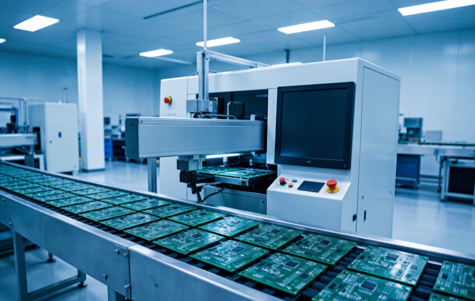
Inspection and test methods are selected according to joint visibility, electrical access and product risk.
Quality is verified through records, not promises.The VeriPCB manufacturing system
Four control stages turn design files into a reviewable and repeatable manufacturing program.
| Stage | What is verified | Customer value |
|---|---|---|
| 01 · Engineering verification | Design files, DFM, stack-up, materials and manufacturing risks | Find ambiguity while change is still inexpensive |
| 02 · Material verification | Base material, copper, finish, exact MPNs and approved alternates | Prevent material and sourcing surprises |
| 03 · Process control | Fabrication route, SMT settings, work instructions and inspection points | Keep samples and recurring builds consistent |
| 04 · Quality verification | Electrical test, AOI, X-ray, functional test and final release by scope | Create evidence for shipment approval |
Manufacturing process
Each step has an input, a control point and a defined output.
Verify revision, stack-up and DFM inputs.
Confirm PCB materials, BOM and sourcing rules.
Control the approved board manufacturing route.
Apply and verify the specified surface finish.
Screen bare boards against agreed requirements.
Run SMT, THT and mixed-technology processes.
Complete agreed inspection and functional checks.
Release configuration, records and packaging.
Industrial focus
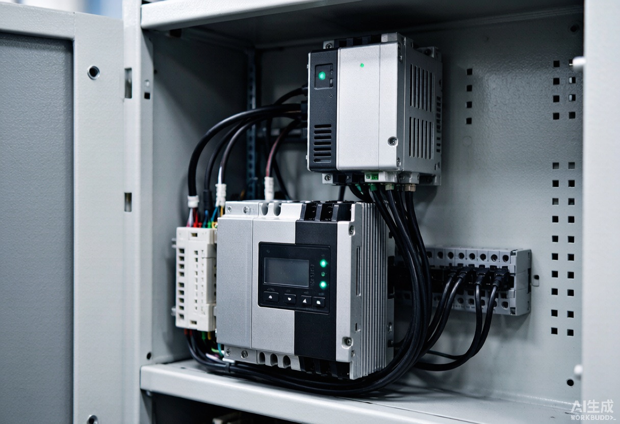
Revision-controlled electronics with long lifecycle and clear testing needs.
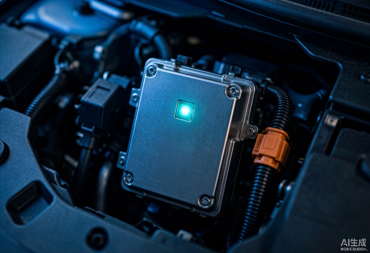
Boards where thermal, current and functional requirements must be reviewed.

High-mix products needing engineering communication and controlled sourcing.
Next step
Share Gerber or ODB++, BOM, centroid, assembly drawings, quantity and test requirements. We will confirm process fit and quotation assumptions before material commitment.